


Séminaire Nano
Mardi 19 Novembre 2019 à 11h00.
2D-0D heterostructures : a new platform for single-electron electronics, spintronics and optoelectronics.
Jean-François Dayen
(IPCMS, Strasbourg)
Salle de séminaire (RdC bât. Lippmann)
Invité(e) par
V. Dupuis
Axe : Nanosciences
présentera en 1 heure :
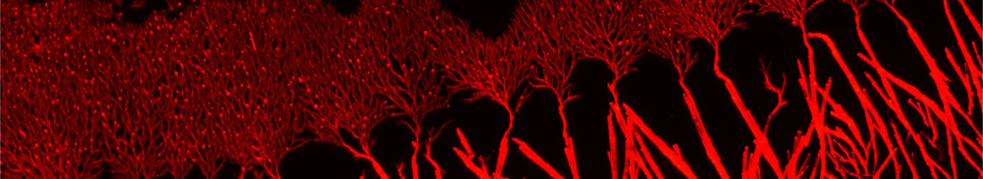
''The rise of graphene, followed by the more recent (re)discovery of the vast family of transition metal dichalcogenides 1, has fueled an unprecedented inter-disciplinary research effort, at the interface between physics, chemistry and engineering. Because of their atomically-thin structure, high surface to volume ratio, and reduced electric screening, new properties and functionalities are expected to emerge when exploiting the interactions of two-dimensional (2D) materials placed in contact with other nanomaterials, including (0D) nanoparticles, molecules, and nanowires.2. These so-called Mixed-dimensional van der Waals Heterostructures (“MWH”) are now at the forefront of basic nanoscience and applied nanotechnology2, providing new sets of possibilities to tailor device functions and novel physical properties.
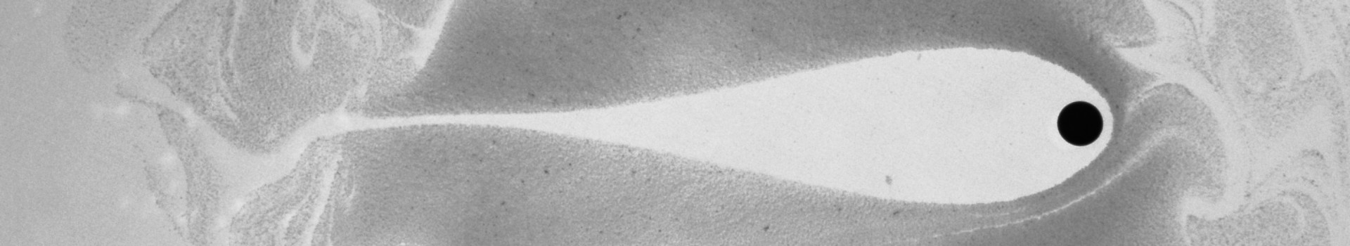
We report a simple and scalable fabrication route of new 2D material/0D clusters heterostructures, exploiting the self-organized growth over graphene of epitaxial flat aluminum based nanoclusters assemblies. Our devices based on Graphene-Aluminum clusters peculiar structure show robust and reproducible features of single-electron transport combined with magnetic functionalities.
We first provide experimental evidence that 2D materials are unique promising alternative to skirt the challenging issue of contacting the nanoparticles one by one with external leads in the sake of developing single electron transport devices 3. Finally, the spintronics properties of 2D–0D heterostructures are unveiled4. An anisotropic magneto‐Coulomb effect, mediated by spin–orbit coupling within a single ferromagnetic electrode, provides tunable spin‐valve‐like magnetoresistance signatures and controllable magnetic modulation of the device's single‐electron charge states, without need of spin coherent tunnelling transport. These heterostructures pave the way towards scalable nanospintronics device architectures at the crossroads of 2D material physics and spin electronics. Depending time remaining, I will end by recent results showing the prospects of 2D/0D systems for reconfigurable photo-transistors.
References :
1. Ferrari, A. C., Bonaccorso, F., Fal’ko, V., et al. Science and technology roadmap for graphene, related two-dimensional crystals, and hybrid systems. Nanoscale 7, 4598 (2015).
2. Jariwala, D., Marks, T. J. & Hersam, M. C. Mixed-dimensional van der Waals heterostructures. Nature Materials. 16, 170 (2017).
3. Godel, F., Mouafo, L. D. N., Froehlicher, G., et al. Conductance Oscillations in a Graphene/Nanocluster Hybrid Material: Toward Large-Area Single-Electron Devices. Advanced Materials. 29, 1604837 (2017).
4. Mouafo, L. D. N., Godel, F., Melinte, G., et al. Anisotropic Magneto-Coulomb Properties of 2D-0D Heterostructure Single Electron Device. Advanced Materials. 30, 1802478 (2018).
''